YouTuber's backyard fab ambitions expand from RAM to homebrew LEDs
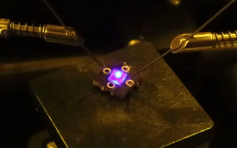
A YouTuber on a mission to liberate semiconductor manufacturing from the grip of multinational megacorporations is back with a new round of DIY success, this time manufacturing working LEDs in his backyard fab.
Dr.
Semiconductor, also known as semiconductor engineer Dr.
Matthew Hartensveld, per his recently launched website, first caught the internet’s attention five months ago when he built a class-100 cleanroom in a shed in his backyard.
Back in April, we wrote about his successful project to build his own DRAM in the clean shed, and the video he posted over the weekend on building his own LEDs follows that project with more ingenious success.
Hartensveld’s decision to construct his own LEDs is directly connected to his RAMbitions, mind you - this isn’t some side project to light stuff up for fun.
As Hartensveld notes in the video’s introduction, working DRAM cells are great, but they’re a far cry from functional DDR5 chips that can be plugged into a computer in lieu of ever-costlier chips from a major manufacturer.
Turning cells into a RAM chip requires a lot more fabrication and packaging work, but there’s a problem there: attaching a finished silicon die to a circuit board requires lining up a whole bunch of tiny contacts with corresponding pads on the board.
Because silicon is opaque to visible light, it takes more work to get everything aligned correctly.
Enter LEDs made with gallium nitride (GaN): GaN is transparent, and LEDs still have to be attached to a circuit board to provide them with power, making them the perfect test bed for home packaging experimentation.
“Not only does gallium nitride LED material help us develop our packaging process, it also helps us make some RGB,” Hartensveld said in the video.
“And everyone knows RGB makes RAM faster … at least emotionally.” Etching GaN into LEDs traditionally requires the use of hazardous chlorine gases, which Hartensveld said in his video made it impractical and unsafe for his purposes - not to mention ridiculously expensive to either build or acquire the equipment necessary to do it safely.
He instead decided to go with a laser etcher, using a 355 nm ultraviolet wavelength that GaN absorbs.
After testing the laser etching process and finding it successful, Hartensveld moved on to a more traditional LED production flow, adding p-type contacts that supply positive charge and n-type contacts that supply negative charge using a typical process of applying photoresist and using metal deposition to fabricate his diodes.
5News aggregated this summary from the outlet’s public feed. The full article, with all the context, is on www.theregister.com — the content belongs to The Register.