Applied Materials’ $5 billion AI lab aims to cut chip development time in half—and restore Silicon Valley’s edge
Silicon Valley has built some of the world’s most impressive and valuable companies, with names like Apple , Alphabet , and Meta , worth trillions of dollars apiece.
When it comes to building the actual facilities where chips, computers, and other game-changing innovations are created, however, America’s tech capital has much less to show.
Most chip facilities are now located overseas or out of state, and the most striking thing about Silicon Valley’s landscape of low-slung buildings and office parks is just how unimposing it is.
That makes what Applied Materials—the world’s largest chipmaking equipment producer—did on Monday so unusual.
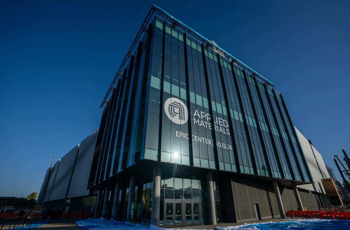
The 59-year-old company officially unveiled its new EPIC semiconductor research and development facility, a two-year construction project located at Applied Materials’ Sunnyvale, Calif. campus, just down the road from its headquarters.
Quite simply: it’s the biggest thing around.
The massive 600,000-square-foot structure of glass, concrete, and steel (two Eiffel Towers’ worth of steel, according to the company), looms over its environment like a spaceship from another world.
The idea behind the facility is equally bold.
The $5 billion EPIC center was built in partnership with some of the world’s top chip industry players, including Intel , TSMC , Micron , SK Hynix, and Samsung .
The companies will each have teams of researchers on-site, working alongside Applied Materials’ engineers and getting early access to Applied Materials’ newest equipment, to develop advances in microprocessors and memory chips.
Applied Materials described EPIC as the largest-ever U.S. investment in advanced semiconductor equipment R&D, with total capital investment expected to reach $5 billion when all is said and done.
The facility’s so-called clean rooms, in which bunny-suit wearing researchers operate machines that etch microscopic circuits into silicon wafers, will occupy the space of three football fields.
Within that space, competing companies—like memory chip companies Micron and SK Hynix—will have their own private test facilities, crammed with advanced chipmaking gear, where they will work directly with dedicated teams from Applied Materials.
“Having innovators co-located together, having earlier access to the technologies that enable new AI architectures, is a complete game changer,” said Applied Materials CEO Gary Dickerson in an interview with Fortune at the event.
5News aggregated this summary from the outlet’s public feed. The full article, with all the context, is on fortune.com — the content belongs to Fortune.