'Beyond human intuition': AI designs chip components 500 times smaller than what engineers could ever imagine
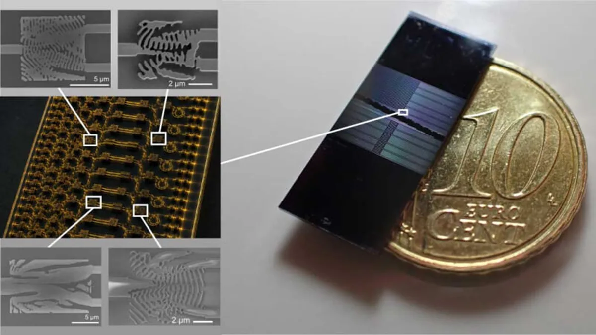
Photonic microchips are around the size of a penny.
This close-up shows computer-designed nanostructures, wavelength splitters, mode sorters and mirrors, while the illustrations on the left show how the components could be integrated into photonic circuits. (Image credit: Tony Bi / MPL ) Scientists have successfully shrunk three components used in photonic microchips by up to 500 times, leaving considerably more space for other on-chip functionality.
The achievement was made possible with an artificial intelligence (AI) algorithm that generated these tiny designs, which the researchers described as "beyond human intuition." Whereas conventional microchips use electrons to transmit and process information, photonic microchips utilize particles of light ( photons ).
They can therefore process and transmit data much faster than electronic chips can, because photons can carry information at the speed of light .
They also offer higher bandwidth, as different wavelengths can carry distinct data streams, and they lose less energy as heat.
As a result, photonic chips are used where fast, high-bandwidth data transmission is essential, such as in fiber-optic communications, data centers, AI, lidar systems for autonomous vehicles, and quantum computing .
Instead of metal wires, micrometer-wide channels called waveguides direct light across the photonic chip.
These chips also contain wavelength splitters, spatial mode sorters and mirrors — all of which are essential for separating and directing different wavelengths and light patterns within a footprint a fraction of the width of a human hair.
In the new study, the scientists used AI-generated designs to fabricate these three components on an ultracompact scale.
They published their findings May 28 in the journal Nature Communications .
The newly available on-chip space could allow engineers to "unlock new functionalities" by packing on more components, the researchers wrote in the study.
Notably, the work demonstrates that AI can produce boundary-pushing chip designs that are also practical to manufacture.
AI worked backward to generate the component designs The researchers started by informing the algorithm exactly what they wanted the components to do to the light and by providing certain manufacturing constraints, such as limits on how sharply the nanostructures could curve The AI algorithm then worked backward, testing and refining different designs until it found the delicate nanostructures that could achieve the desired result.
"Inverse design lets us define what we want light to do, and the optimization finds a structure that does it, often one no human would have drawn," study first author Toby Bi , a researcher at the Max Planck Institute for the Science of Light, said in a statement .
5News aggregated this summary from the outlet’s public feed. The full article, with all the context, is on www.livescience.com — the content belongs to Live Science.